The storage decision is usually made once, early, and then lived with for the life of the product. Changing it later means a board revision, a new boot configuration and a fresh software validation campaign.
Three options cover most embedded designs: raw NAND flash, eMMC and UFS. They are not simply three points on a speed scale. They differ in who manages the flash, how the processor talks to it, and what happens when a block eventually wears out.
The three options in one paragraph each
Raw NAND is the bare flash die. The processor, or a controller in the processor, must handle error correction, bad block management, wear levelling and the file system. It is the cheapest per gigabyte and the most demanding to design with.
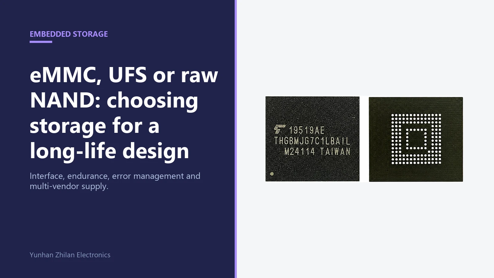
eMMC puts the NAND die and a managed controller into one BGA package with a standard parallel interface. The controller hides bad blocks, performs error correction and wear levelling, and exposes a simple block device. It is the workhorse of embedded storage.
UFS is the successor architecture: the same managed-controller idea, but with a serial, full-duplex, command-queuing interface. It delivers several times the throughput of eMMC, at a higher price and with more demanding board design requirements.
Representative parts: KIOXIA 16GB eMMC, Samsung 64GB eMMC and FORESEE 64GB eMMC for managed designs, and Micron industrial-temperature eMMC where the operating range is the deciding factor.
Comparison table
| Factor | Raw NAND | eMMC | UFS |
|---|---|---|---|
| Interface | Parallel or serial NAND bus, with control and status lines | Parallel bus: command, clock, data, plus boot and reset | Serial, full duplex, differential lanes plus reference clock |
| Typical sequential read | Depends heavily on the controller | Around 200-400 MB/s for current mainstream parts | Around 800-2,000 MB/s or more |
| Command queueing | No | No; effectively one outstanding operation | Yes; multiple commands in flight |
| Who manages bad blocks | You, in software or in the SoC's NAND controller | The built-in controller | The built-in controller |
| Error correction | Your responsibility; ECC strength must match the die | Handled internally | Handled internally |
| Wear levelling | Your responsibility | Handled internally | Handled internally |
| Pin count and layout | Moderate, but timing-critical | Moderate, with length-matched groups | High; differential pairs and impedance control required |
| Boot support | Via the SoC's NAND boot path | Standard eMMC boot partitions | Standard UFS boot support on modern SoCs |
| Cost per GB | Lowest | Low | Higher |
| Lifecycle and availability | Long, multi-vendor, but die revisions move fast | Long, many vendors, wide capacity range | Shorter history; flagship mobile driven |
| Typical use | Cost-driven consumer, very high volume, simple firmware | Industrial control, HMI, automotive infotainment, IoT gateways | Phones, tablets, high-performance embedded, AI edge devices |
When eMMC is the right answer
eMMC remains the default for industrial and embedded designs, and the reason is not speed. It is the combination of a simple interface, a managed flash stack and a very wide supplier base.
1. The processor has an eMMC interface and you do not want to write a flash driver
Most SoCs used in industrial products boot directly from eMMC. The operating system sees a block device, a file system goes on top, and the design is finished. No error correction tuning, no bad block table, no wear levelling code to validate.
2. Multiple vendors must be able to supply the same socket
eMMC is standardised enough that parts from different vendors are pin-compatible for a given package and ball-out. Qualification is still required, but having three sources for a ten-year product is a commercial advantage that raw NAND rarely offers and UFS often does not.
3. The application needs less than a few hundred megabytes per second
Control panels, data loggers, gateways, motor drives, medical instruments and point-of-sale terminals almost never saturate eMMC bandwidth. Buying UFS for these products means paying for performance that the product cannot use.
4. Industrial temperature grade and long lifecycle matter
Industrial and automotive eMMC parts are available in extended temperature grades with defined long-term supply commitments. That combination is much easier to secure in eMMC than in the UFS market, which is driven by mobile flagship cycles.
When UFS is the right answer
UFS earns its cost when throughput, latency under mixed load, or concurrency genuinely limits the product.
- High-resolution video capture or playback at the edge, where sustained write bandwidth is the bottleneck.
- Machine vision and AI inference at the edge, where models and image buffers are read continuously and the storage must keep up with the accelerator.
- Multi-application devices that must serve several data streams at once; command queueing is the difference between a responsive system and a stuttering one.
- Products where the storage is also the user experience, such as handheld instruments that boot and load datasets in front of the operator.
The costs are real: UFS requires careful impedance-controlled routing, a reference clock, and a SoC that supports the interface. It also ties the design more closely to whichever vendors still make the capacity and grade you selected.
When raw NAND still makes sense
Raw NAND survives in two situations: extreme cost pressure at very high volume, and designs where the SoC has a mature hardware NAND controller and the firmware team is comfortable managing it.
Be realistic about the hidden cost. Error correction strength must be matched to the die generation, bad block management has to survive power loss, and wear levelling has to be validated. Those requirements do not disappear because the die was cheaper.
Endurance: how to size the part
Endurance is expressed in program and erase cycles, or in terabytes written for the whole device. What matters for sizing is the daily write volume, not the total capacity.
- Estimate the bytes written per day in normal operation, including logs, databases and temporary files.
- Add the write amplification introduced by the file system and by the application's write pattern.
- Add the firmware update path: an update that rewrites a large partition is a significant share of the lifetime budget.
- Multiply by the expected service life in days, then add a safety factor for field behaviour that differs from the bench.
A design that writes a log file every second will wear out storage far faster than a product that writes the same total volume in large, infrequent blocks. Write pattern matters as much as write volume.
Mistakes that show up in the field
- Uncontrolled power loss. Sudden power removal during a write is the most common cause of a corrupted file system on managed storage. Either design for controlled shutdown or choose parts with robust power-loss handling and verify it.
- Treating eMMC as though it cannot wear out. Managed flash still has a finite lifetime. Writing logs continuously for years will end it.
- Choosing capacity by price only. Larger capacity spreads wear across more blocks, so a slightly larger part can outlive a cheaper smaller one.
- Ignoring the temperature grade. Commercial-grade storage in an enclosure that reaches 70 °C internally will not meet its rated endurance.
- Assuming a drop-in replacement is drop-in. Two eMMC parts with the same capacity and package can differ in boot partition behaviour, timing and power-up requirements.
A short decision path
- Does the processor support UFS, and does the application actually need more than roughly 300 MB/s? If yes to both, evaluate UFS.
- Does the product need multiple qualified sources and a long lifecycle at moderate bandwidth? If yes, choose eMMC.
- Is the SoC's NAND controller mature, the firmware team experienced, and the volume high enough that the die cost dominates? If yes, raw NAND is defensible.
- In every case, size endurance from the real daily write volume before fixing the capacity.
How we can help
Send us the capacity, the temperature grade, the package and the interface you need, and we will come back with the parts we can supply and their availability. If you are replacing a discontinued part, include the original number and we will check package and boot compatibility, not just capacity.
For production planning, tell us the annual volume and the target service life. Storage is one of the few components where the correct answer changes with the write pattern rather than with the datasheet alone.


